



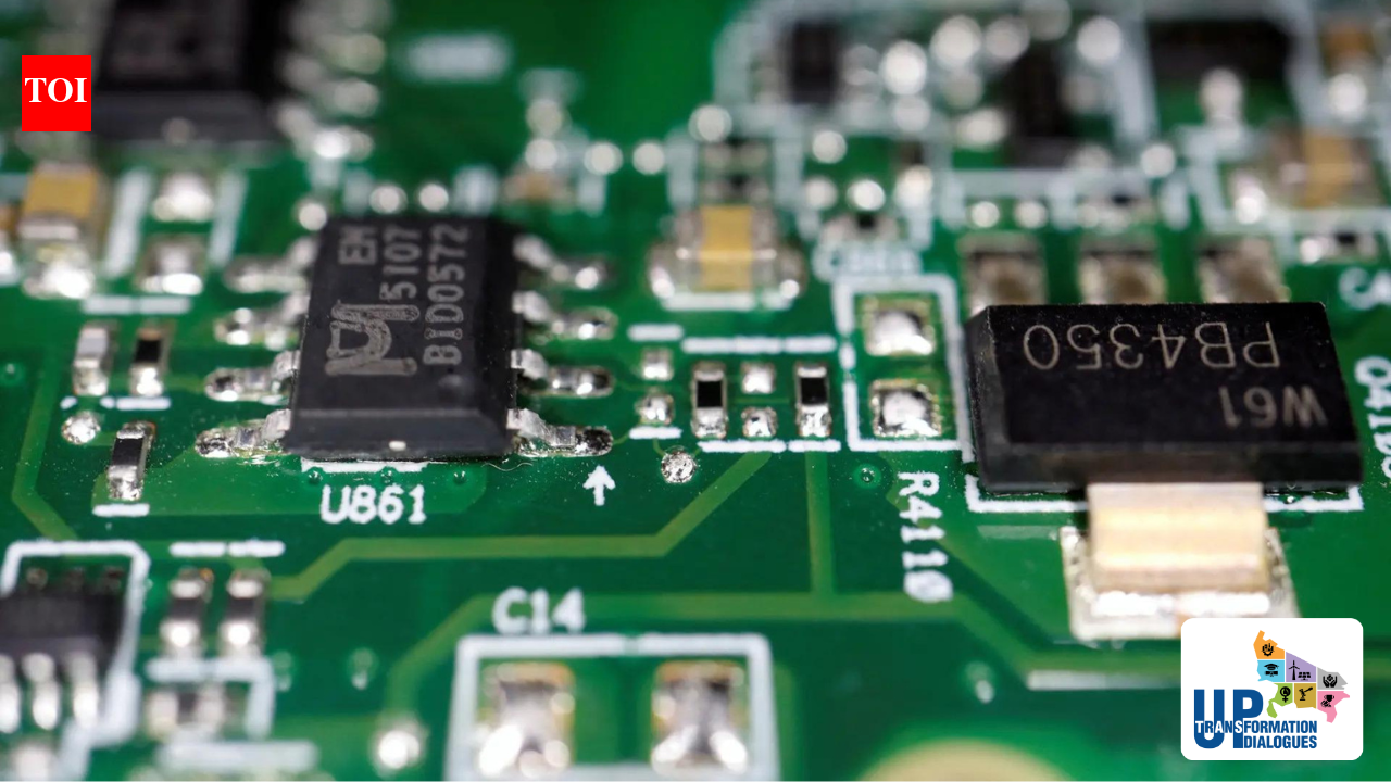
The Uttar Pradesh Semiconductor Policy, 2024 is a bold, flagship initiative by the Uttar Pradesh Government to establish the state as a leading semiconductor and advanced electronics manufacturing hub in India. It seamlessly complements the national India Semiconductor Mission (ISM) and supports the Yogi Government’s vision of becoming a $1 trillion economy by attracting high-value, technology-intensive investments.
Objectives
– Build a world-class semiconductor ecosystem with state-of-the-art infrastructure and global supply chain integration.– Attract large-scale investments in semiconductor fabrication (Fab), ATMP/OSAT, display manufacturing, compound semiconductors, silicon photonics, sensors, and discrete devices.– Create high-skilled, high-wage employment opportunities.– Foster research, innovation, design, and startups in semiconductors.– Position Uttar Pradesh as a preferred global destination for advanced electronics manufacturing.
Policy duration
Effective for five years from the date of notification in 2024 (or until superseded).Focus Areas– Semiconductor fabrication units– ATMP (Assembly, Testing, Marking & Packaging) and OSAT facilities– Display fabrication– Compound semiconductors and silicon photonics– Sensors and discrete semiconductors– Semiconductor design, R&D, and innovation centres
Incentives
Capital Subsidy: Up to 50 per cent additional capital subsidy on the central government’s incentive (subject to caps), making it one of the most competitive offers in India.Land & Infrastructure: Concessional land in semiconductor parks/clusters, plug-and-play infrastructure, reliable power, water, and logistics support.
Tax & duty benefits:
– Up to 100 per cent stamp duty exemption– Concessional electricity tariffs and duty exemptions– SGST exemptions (up to 10 years in recent amendments)– Interest subsidies and other operational supportSkill Development & R&D: Partnerships with universities, Centres of Excellence, incubation centres, and targeted skilling programmes.Ease of Doing Business: Single-window clearance, dedicated relationship managers, and time-bound approvals.Strategic Locations: Focus on Noida, Greater Noida, and YEIDA region (Yamuna Expressway Industrial Development Authority), leveraging proximity to the new Noida International Airport, expressways, and the Delhi-Mumbai Industrial Corridor.
Results as of now
The policy has rapidly gained momentum and is delivering tangible results with a major investment of about Rs 3700 crore by HCL-Foxconn JV (India Chip Private Limited) in YEIDA Sector 28, Jewar(near Noida International Airport). It will produce display driver chips (capacity: ~20,000 wafers/month, 36 million chips/month) for smartphones, laptops, automotive, and other electronics. The project has received Union Cabinet approval, land allocation (48 acres), and groundbreaking has taken place, with commercial production targeted for 2027. It is expected to generate over 2,000 direct and indirect high-skilled jobs.Investment in Pipeline: Early proposals under the policy totalled over Rs 32,000–40,000 crore, with multiple projects in advanced stages of consideration and approval. The state continues to attract interest from global and domestic players in OSAT, compound semiconductors, and electronics manufacturing.In fact, Yamuna Expressway Industrial Development Authority (YEIDA ) has emerged as Uttar Pradesh’s premier semiconductor hub. Initiatives include developing an Electronics Manufacturing Cluster (EMC Park) and supporting infrastructure. Policy amendments in 2025–2026 have made incentives even more investor-friendly (e.g., targeted support for large projects Rs 3,000 crore). These projects are catalysing thousands of direct high-skilled jobs and tens of thousands of indirect opportunities across the value chain — from design and R&D to logistics and ancillary industries.Uttar Pradesh is transitioning from a negligible presence to a credible player in India’s semiconductor journey, strengthening domestic supply chains and reducing import dependence. The expected Long-Term Impact is to attract cumulative investments worth tens of thousands of crores in the coming years, establish Uttar Pradesh as a core node in India’s semiconductor and electronics ecosystem, boost exports of high-value electronic products, drive innovation, skilling, and sustainable industrial growth and contribute significantly to the state’s $1 trillion economy goal.The Uttar Pradesh Semiconductor Policy, 2024, combined with proactive implementation, land allocation, and central-state collaboration, is delivering early wins and positioning the state as one of India’s fastest-rising advanced manufacturing destinations. With continued momentum in YEIDA and beyond, Uttar Pradesh is well on its way to becoming a ‘semiconductor powerhouse’ in the next decade.


