



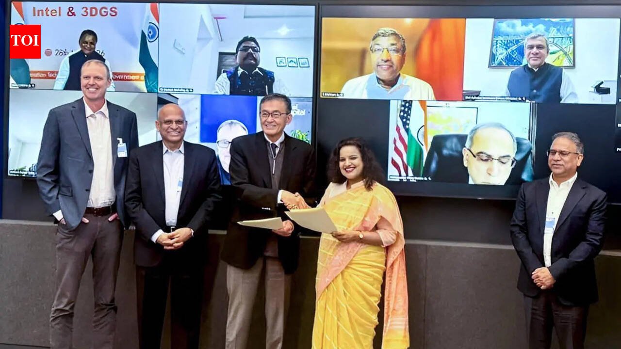
Bhubaneswar: Odisha govt on Friday signed a memorandum of understanding (MoU) with tech major Intel Corporation and 3DGS Inc USA to bring substrate manufacturing technology to India, Union electronics and IT minister Ashwini Vaishnaw said.The project, with an estimated investment of approximately US$ 3.3 billion (more than Rs 31,600 crore) in Bhubaneswar, represents one of the largest high-technology manufacturing investments in the country, a govt statement said.Vaishnaw, in a social media post, wrote, “This will further advance semiconductor ecosystem in India.” The Union minister along with CM Mohan Charan Majhi and CEO, Intel, Lip-Bu Tan witnessed the MoU signing by officials digitally.Vaishnaw said the landmark pact aligns with the Centre’s vision to build a comprehensive semiconductor ecosystem. The project will be implemented in phases over 5-6 years and is expected to generate over 1,800 direct high-skilled jobs, besides significant indirect employment, the statement added.The proposed facility will focus on advanced packaging glass core substrates and high-density interconnect substrates, with Intel providing technology know-how and process expertise. It is expected to boost capability development, ecosystem growth and export-oriented manufacturing.The initiative complements ongoing efforts under the India Semiconductor Mission to strengthen domestic manufacturing, design capabilities and supply chains, and could position Odisha among emerging global semiconductor hubs.Substrate manufacturing involves producing base materials for microchip fabrication and packaging, including silicon wafers and capabilities in this segment and is a leader in next-generation packaging technologies.With conventional transistor scaling nearing its limits, innovation in advanced packaging and substrate design has become critical to enhancing performance and energy efficiency, especially in artificial intelligence, computing and communications. Such technologies are key to building resilient and self-reliant semiconductor ecosystems.Following Union cabinet approval in August last year, 3DGS is setting up a vertically integrated advanced packaging and embedded glass substrate facility at Info Valley in Bhubaneswar with a proposed investment of Rs 1,943 crore. The plant will bring advanced capabilities, including glass interposers with integrated passives, silicon bridges and 3D heterogeneous integration (3DHI) modules.The development comes amid India’s push to strengthen its semiconductor ecosystem, with the Centre approving 12 projects under the India Semiconductor Mission involving investments of about Rs 1.64 lakh crore.


